eSi-3250
32-bit RISC IP, High-Performance CPU
Our eSi-3250 32-bit RISC IP core is a high-performance processor ideal for integration into ASIC and/or FPGA designs requiring caching, due to the use of slow on-chip memories such as eFlash, off-chip memories, or where the CPU core to bus clock ratio is greater than 1. 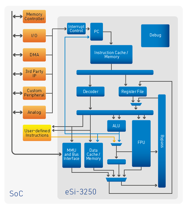
Download Documents
32-bit RISC IP: eSi-3250 Technical Overview
Features
- 32-bit RISC architecture
- 16 or 32 general purpose registers
- 104 basic instructions and 10 addressing modes
- Optional IEEE 754 floating point unit (FPU)
- Supports up to 74 user-defined instructions
- 5-stage pipeline
- Optional memory management unit (MMU)
- Configurable instruction and data caches (1-64kB, direct mapped or 2 or 4 way associative)
- AMBA AXI or AHB interconnect and APB peripheral bus
- User and supervisor modes
- Up to 32 vectored interrupts plus NMI and system call
- HW nested and prioritizable interrupts
- Fast interrupt response time of 6-9 cycles
- JTAG or serial debug, with optional trace and performance counters
- Up to 4.12 CoreMark per MHz
- Multiprocessor support
- Intermixed 16 and 32-bit instructions result in exceptional code density without compromising performance
- ASIC performance (Typical 28nm):
- Up to 1 GHz
- From 17k gates
- From 4uW/MHz
- High quality IP:
- Verilog RTL
- DFT ready
- Silicon proven
- C and C++ software development using license-free toolchain, under industry standard Eclipse IDE
- Easy migration path to cacheless version
Architecture
The eSi-3250 32-bit CPU is targeted specifically for applications with high performance requiring caching, due to the use of slow on-chip memories such as eFlash, off-chip memories, or core/bus ratios greater than 1.
A triple core eSi-3250 with FP
The processor features separate instruction and data caches that can be configured in size (from 1- 64kB) and associativity (direct mapped, 2 or 4-way associative) to increase performance and reduce power. The optional paged memory management unit (MMU) enables the implementation of virtual memory or memory protection. The 5-stage pipeline allows GHz clock frequencies to be achieved.
The eSi-3250’s instruction set includes everything you would expect in a high-performance processor. There are a number of optional application specific instructions and addressing modes. For example, a set of IEEE-754 compliant single-precision floating point instructions are available. Integer arithmetic instructions include a full 64 multiply and accumulate and divide. Bit manipulation instructions such as bitfield extract and insert, count leading zeros, population count, find first set and bit reverse can be included. Integer square root, absolute value, min/max, CRC and parity are also available. 32-bit SIMD instructions with 16-bit elements exploit data parallelism and reduce loop counts. Wait-for-interrupt instructions allow fast entry to low power states, enabling clock and power gating.
For those applications that require extreme performance or ultra low power operation, user-defined instructions and registers can be implemented.
Instructions are encoded in either 16 or 32-bits, with all of the commonly used instructions being encoded in 16-bits, maximizing code density and improving cache performance.
The processor supports both user and supervisor operating modes, with privileged instructions and memory areas, to allow an O/S kernel to be fully protected from user applications.
Hardware debug facilities include hardware breakpoints, watchpoints, trace, performance counters, null pointer detection and single-stepping for fast debugging of ROM, FLASH and RAM based programs.
Toolchain
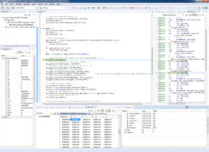
Eclipse Debugger
The toolchain is based upon the industry standard GNU toolchain, which includes an optimising C and C++ compiler, assembler, linker with LTO, debugger, simulator and binary utilities. All these tools can be driven by the customizable Eclipse IDE or from the command line.
The debugger can connect to HW targets via a low-cost USB- JTAG adapator or serial link and RTL simulations via a Verilog PLI library.
Complete C and C++ libraries are supplied. Ports of Micrium’s uC/OS-II RTOS,Express Logic’s ThreadX, FreeRTOS and the lwIP TCP/IP stack are available.
The toolchain is available for both Windows and Linux hosts and is available to use at no cost.
IP Delivery
The eSi-3250 is delivered as a Verilog RTL IP core. The design is target technology independent and DFT ready, supporting full scan insertion for all flip flops and memory BIST. Example scripts are provided for popular EDA tools.
A selection of AMBA peripherals can be integrated with the core, including: UART, SPI, I2C, I2S, Timer, PWM, Watchdog, GPIO, PS/2, CRC, Ethernet MAC, FIFO, Scatter-Gather DMA, AES, SHA256, quad-SPI flash, static RAM, parallel flash, embedded flash and LPDDR controllers. By using an industry standard bus, a wide range of 3rd party IP cores are compatible with the eSi-3250.
The eSi-SoC tool can generate a multilayer AHB matrix and APB bus to connect the eSi-3250 CPU, memory and peripherals, according to a customer’s specification.